Semiconductor Failure Analysis
Sample preparation by cleaving is used in semiconductor failure analysis and quality control laboratories. The key applications include*:
- Preparation of cross sections for analysis by scanning electron microscopy (SEM).
- Downsizing of full wafers and pieces for electrical probing, surface analysis or further processing.
The cleaving methodology depends on a number of factors including:
- Will the final sample be viewed in the SEM and does the SEM have sample height limitations?
- What target accuracy and repeatability is required.
- Substrate thickness, thickness and materials on the surface.
- Crystal structure of the substrate ((100), (111))
- Orientation of the lithography relative to the substrate (rotated lithography on (100) silicon)
*A good reference document for semiconductor applications is found in the Microelectronics Failure Analysis Desk reference, Seventh Edition. Tejinder Gandhi, editor DOI:10.31399/asm.tb.mfadr7.t91110402
Preparation of samples for SEM
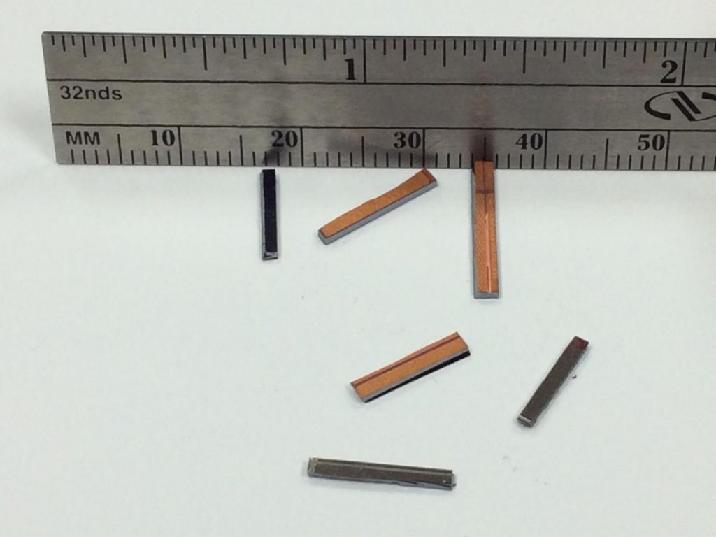
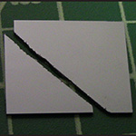
On the right is a 4x3mm sample. It was downsized from 10x10mm in preparation to be viewed in a SEM with sample height restrictions. This is common requirement for SEMs with immersion lenses. CLICK to see the applications note and movie. The movie shows the downsizing process which keeps the SEM area of interest clean.
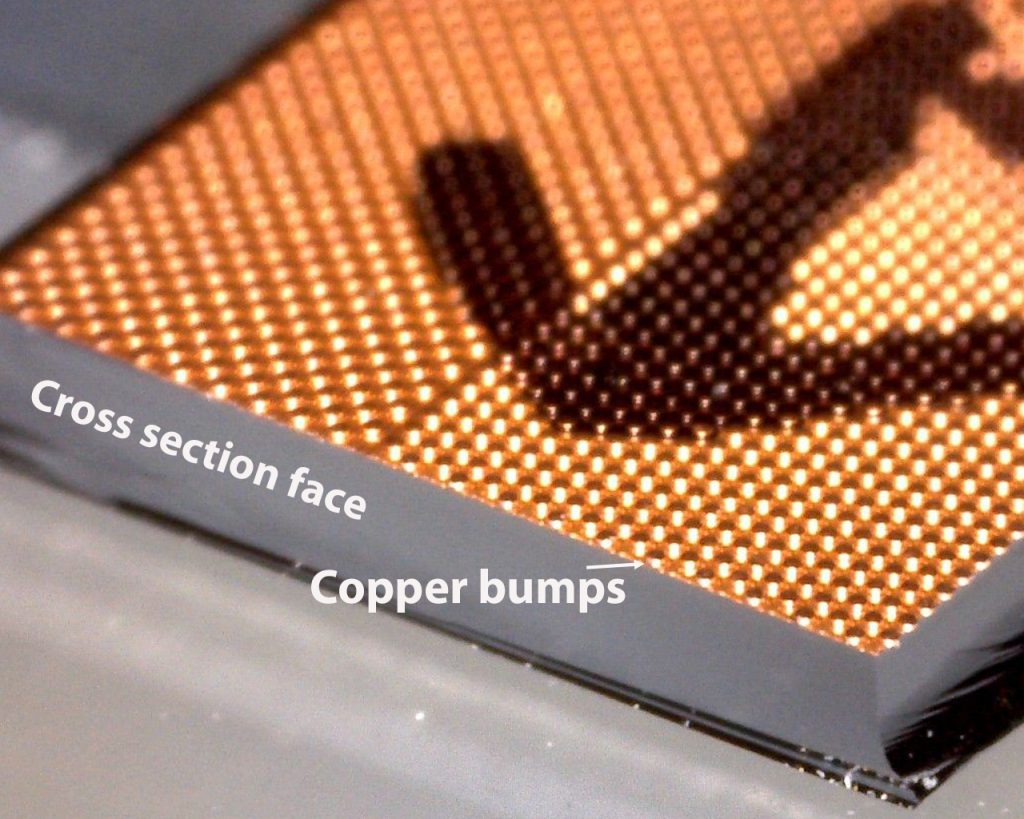
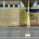
On the far right is a SEM image of a memory structure directly after cleaving. Note that backend structures containing metal will commonly need to be "polished" with an ion mill before fine structures can be resolved in the SEM. Go to the publications section and download the paper "From Transistors to Bumps..."
Downsizing samples for analysis or processing
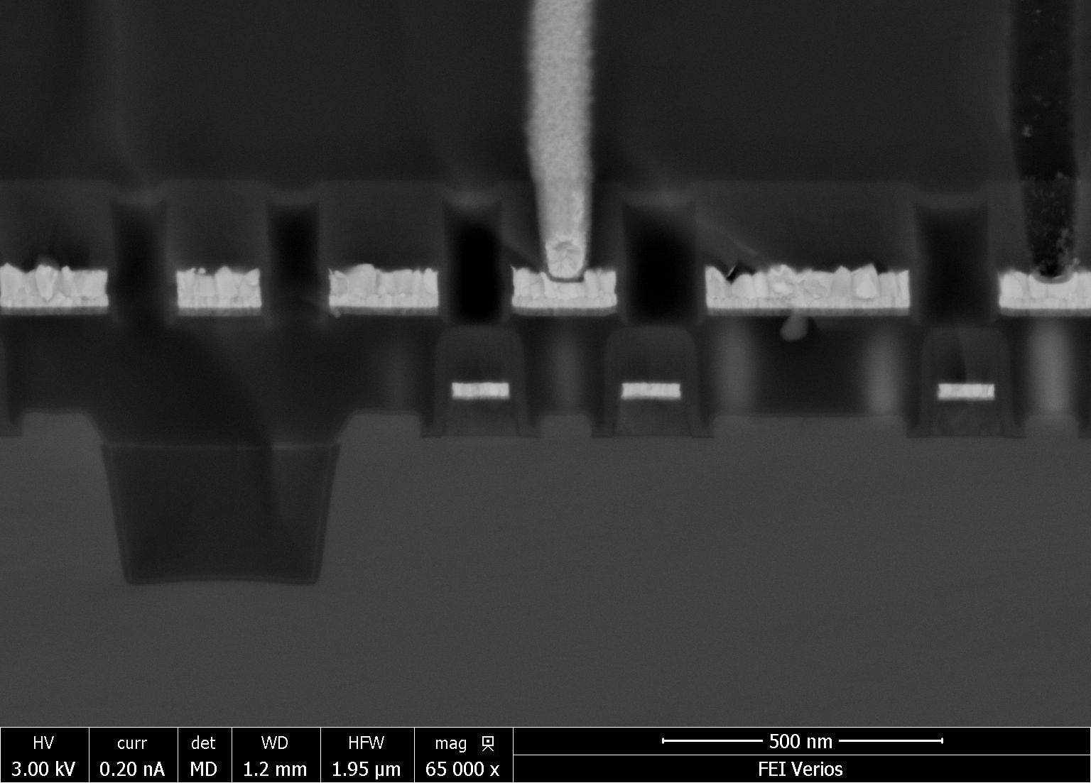
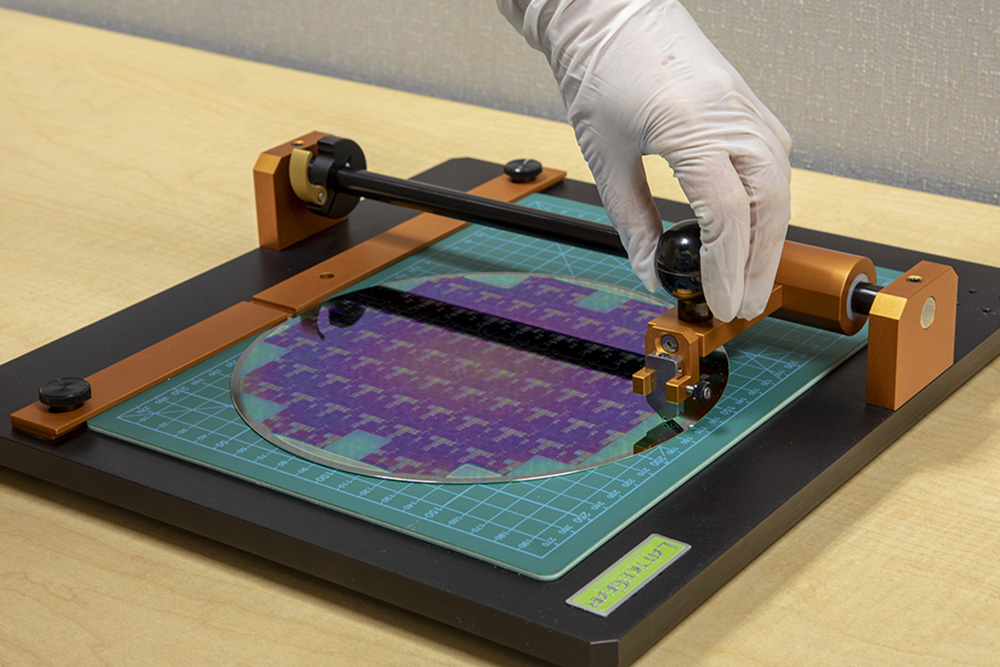
In addition to downsizing wafers to die sized pieces, the LatticeAx is used for thin, small and even off crystal axis cleaving. The image on the right shows the diamond wedge indenter of the LatticeAx precisely positioned on the sample to control the location of the cleave. As the indenter is lowered it creates a defect on the sample surface that eventually causes a cleave to propagate. This method is called "indent to cleave" and can be used on silicon, GaAs and other crystalline, thin samples. Read more about this application HERE
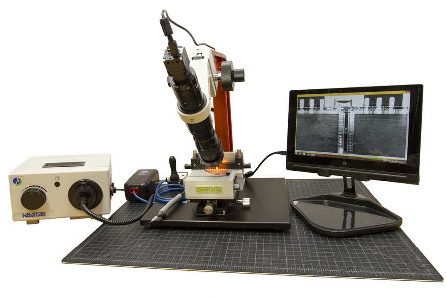
On the far right is an image of a (100) silicon sample cleaved using the FlipScribe. The FlipScribe scribes the sample with a diamond scribe on its backside. This means the scribe never touches the fragile features on the front side. If your samples is large >1"/25mm it best practice to downsize the sample with the FlexScribe and then perform the final downsizing with the FlipScribe.
Solutions
The solution may require one or more tools to get the job done. For instance:
- When accuracy is not the primary consideration downsizing large thin wafers up to 300mm is done easily with the FlexScribe.
- For preparing samples that must have mirror finish facets for photonics or SEM analysis. Downsize with the FlexScribe or FlipScribe and make the final cleave with the LatticeAx.
- Preparing samples that have sensitive thin films on the surface. Use the FlipScribe backside scriber to downsize the samples. Make the final cleave using the LatticeAx to obtain mirror finish facets.
- View publications below that address MEMS decap, cleaving nanostructures, cleaving in the cleanroom and provide general information about cleaving semiconductor materials.
Don't see your application here, CONTACT US for a recommendation.
Products for Semiconductor Applications
Based on your application LatticeGear can recommend the right tool set. Please contact us!

Cleaving Tools
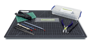
There are a number of accessories that will be important for your laboratory.
CleanBreak Pliers with 3 Sets of Jaws. After scribing you will need to cleave your sample. It is possible to cleave over a sharp edge but the pliers provide symmetrical force when cleaving the sample. Cleanbreak pliers are used for samples 20mm/.75" and larger.
Videos
Watch videos showing the operation of the scribing and cleaving tools and systems.
Semiconductor Publications
Publications (for copies, contact lg@latticegear.com) or for downloadable copies of these publications you must be registered and signed in
