III-V Substrates
Cleaving III-V substrates is simple with the right tools. Applications fit in two major categories.
- Downsizing of full wafers and pieces for surface analysis or further processing..
- Cleaving to make laser bars and edge emitting lasers.
Cleaving GaAs Wafers and Laser Bars
The FlexScribe is commonly used for downsizing wafers. Matt Kim of QuantTera has developed a reliable way to quickly make 5x5 mm die from 4 and 6" wafers. These die are then processed individually saving cost and accelerating time to results. Download the applications note.
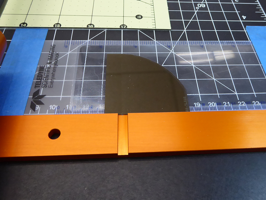
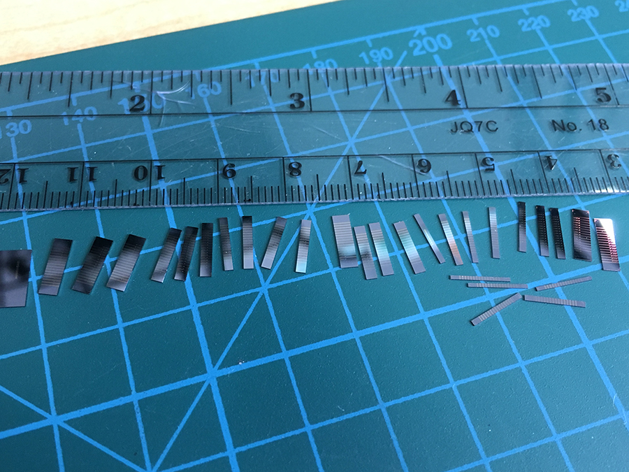
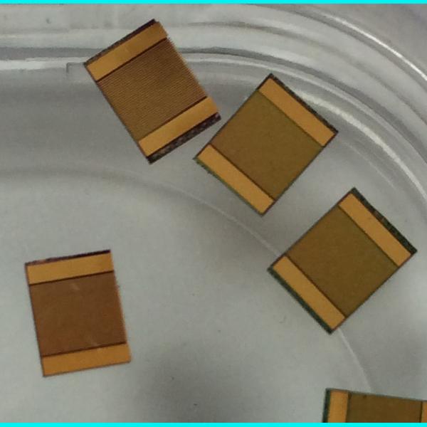
The LatticeAx 420 was used to separate laser bars from a GaAs chip. Both "indent to cleave" and manual methods were used to cleave the GaAs laser bars.
GaN Wafer Downsizing
For III-V substrates and wafers that are cubic such as GaAs and InP, brittle and relatively soft on the mohs hardness scale, cleaving is simple. The LatticeAx alone, does a great job downsizing these materials. It is clean, dry and fast.
For materials that are not cubic or need to be cleaved counter to a crystal plane, tools that can scribe across the entire length of the sample are required. Have a look at the Sapphire page for an explanation. You will need the FlipScribe or FlexScribe to make full length scribes and cleave wafers with hexagonal and trigonal structures. Examples of these materials are GaN, AlN, SiC and Sapphire.
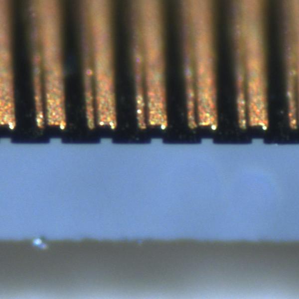
The images on the right are from a 2” GaN wafer. Scribing was done with the FlipScribe and the FlexScribe. The FlexScribe was used to downsize the whole wafer in half. The FlipScribe was used to further downsize by scribing the backside of the wafer, eliminating contamination to the top surface. The combination of frontside and backside scribing give the user flexibility to develop a process for wafers with non-cubic structures. Cleanbreak cleaving pliers were used after scribing to cleave.
Preparation of samples measurement of photonic properties
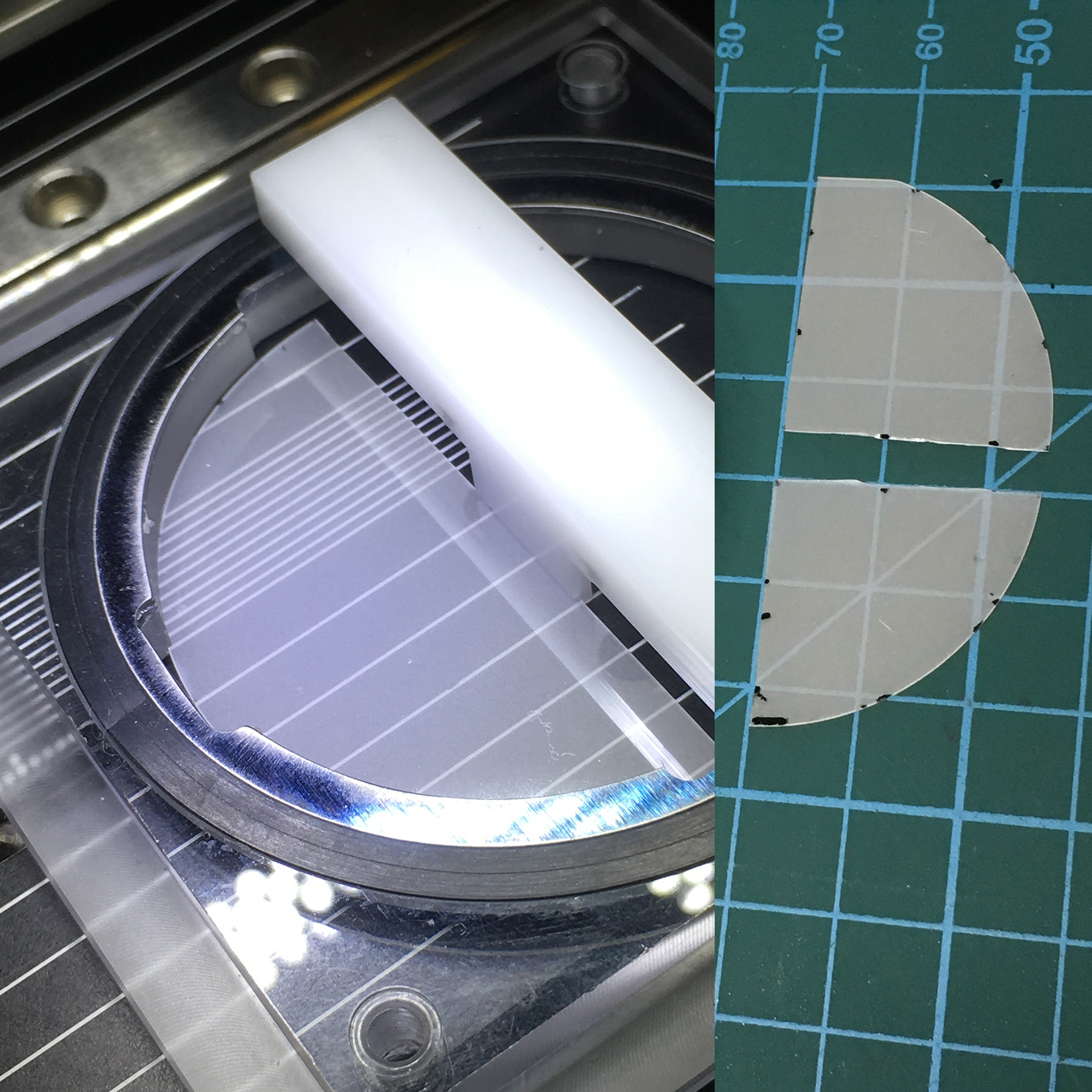
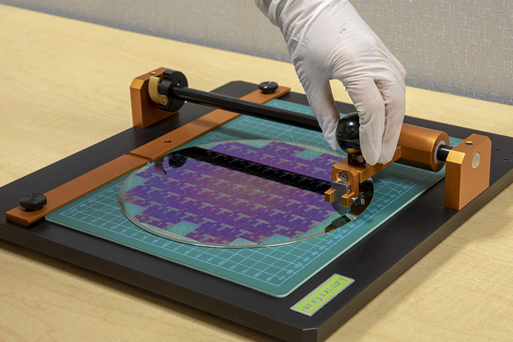
The sample is a 200 μm thin InP wafer with multiple layers of epitaxial films consisting of Al, Ga, In and As. During R&D, a quick, precise means to singulate a die is required to replace dicing by sawing.
The LatticeAx 420 indent to cleave process resulted in rapid, accurate and repeatable singulation.
Downsizing samples for analysis or processing
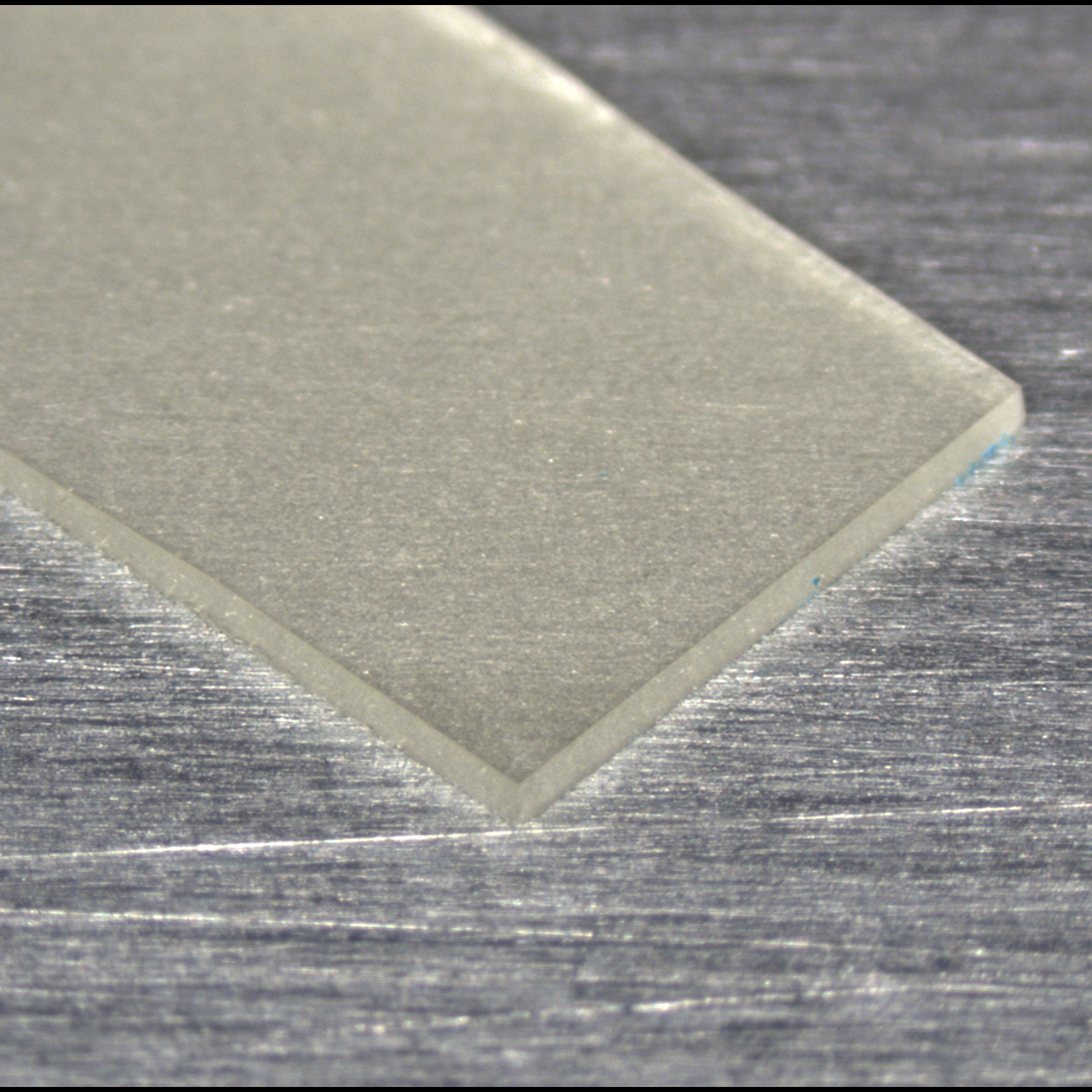
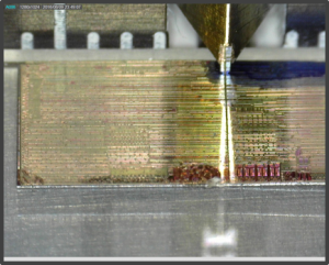
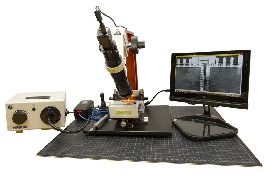
In addition to downsizing wafers to die sized pieces the LatticeAx is used for thin, small and even off crystal axis cleaving. The image on the right shows the diamond wedge indenter of the LatticeAx precisely positioned on the sample to control the location of the cleave. As the indenter is lowered it creates a defect on the sample surface that eventually causes a cleave to propagate. This method is called "indent to cleave" and can be used on silicon, GaAs and other crystalline, thin samples. Read more about this application HERE
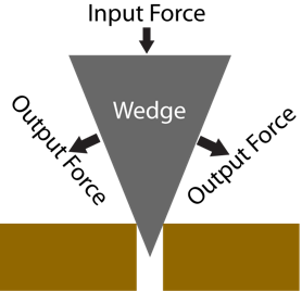
On the far right is shows how the LatticeAx indenter is used as a wedge. The indenter first makes a weak point on the sample surface followed by downward force to cleave the sample.
The solution may require one or more tools to get the job done. For instance:
- When accuracy is not the primary consideration downsizing large thin wafers up to 300mm is done easily with the FlexScribe.
- For preparing samples that must have mirror finish facets for photonics or SEM analysis. Downsize with the FlexScribe or FlipScribe and make the final cleave with the LatticeAx.
- Preparing samples that have sensitive thin films on the surface. Use the FlipScribe backside scriber to downsize the samples. Make the final cleave using the LatticeAx to obtain mirror finish facets.
Don't see your application here, CONTACT US for a recommendation.
Products for III-V Substrates

Cleaving Tools
Ther are a number of accessories that will be important for your laboratory.
CleanBreak Pliers with 3 Sets of Jaws. Once you have an accurate indent or scribe, you will need to cleave your sample. The pliers provide symmetrical force when cleaving the sample. Cleanbreak pliers are used for samples 20mm/.75" and larger.
Videos
Watch videos showing the operation of the scribing and cleaving tools and systems.
Publications
Publications (for copies, contact lg@latticegear.com) or for downloadable copies of these publications you must be registered and signed in
